
Industrial economic development expert Joshua Fairbourne sits down with Luca Calaraili, a veteran in large-scale construction and innovative design, to discuss the ambitious $226 million semiconductor project currently unfolding at Texas A&M. With the global chip race intensifying, this facility represents a pivotal shift in how academic institutions integrate with industrial manufacturing chains. Calaraili, known for his deep understanding of high-tech infrastructure, explores the technical complexities of building “clean room” environments and the strategic importance of the Rellis campus in Bryan, Texas. This conversation delves into the intersection of advanced engineering, state-level capital investment, and the creation of a specialized workforce capable of sustaining the next generation of microdevice fabrication.
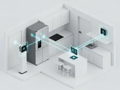
The new facility features Class 100 and 1000 clean rooms equipped with 300mm machinery. How does this specific infrastructure support full-scale production R&D, and what technical challenges arise when integrating metrology, photonics, and radio frequency labs within a single 80,000-square-foot site?
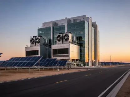
Integrating such diverse technological disciplines into an 80,000-square-foot footprint requires an incredible level of architectural precision and environmental control. The Class 100 and 1000 clean rooms provide the hyper-sterile environments necessary for 300mm machinery, which is the industry standard for high-volume semiconductor manufacturing. When you combine metrology, photonics, and radio frequency labs in one site, the primary challenge is managing electromagnetic interference and vibration isolation, as the sensitivity of these tools is off the charts. We are essentially building a microscopic-scale city where every air molecule and floor tremor is monitored to ensure that research can transition seamlessly into full-scale production. It is a high-stakes balancing act of hazardous materials handling, specialized storage, and complex distribution systems that must function perfectly 24/7.
Flexible labs are designed to mirror real-world production environments for hands-on workforce training. What specific skilled-trade certifications will this site prioritize, and how do you envision students transitioning from these clean rooms directly into high-paying roles at major semiconductor firms?
The beauty of these flexible labs is that they aren’t just theoretical classrooms; they are mirror images of the fabrication floors used by industry giants. We are prioritizing certifications in process and tooling development, testing, and evaluation, which are the backbone of the semiconductor supply chain. By training in these exact clean room environments, students develop the “muscle memory” of a professional technician, making them immediate assets for firms like Samsung or Tokyo Electron America. This hands-on immersion bridges the gap between a degree and a career, allowing individuals to step out of the university and straight into high-demand roles that form the economic heart of the region.
The Rellis campus houses various initiatives ranging from national security to AI hypercomputing. How will the semiconductor institute leverage these neighboring resources, and in what ways does this proximity accelerate the development of advanced microdevices for energy reliability and transportation innovation?
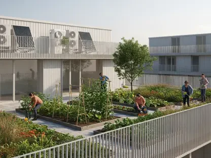
The 3,300-acre Rellis campus is a powerhouse of synergy, where the semiconductor institute acts as the hardware foundation for the neighboring AI and national security hubs. When your chip designers are just a short distance from experts in AI hypercomputing and energy reliability, the feedback loop for innovation becomes incredibly fast. This proximity allows for real-time testing of microdevices in transportation innovation and defense applications, effectively turning the campus into a living laboratory. We aren’t just making chips in a vacuum; we are developing the specific silicon components that will power more reliable energy grids and smarter autonomous vehicles.
With over $226 million allocated for the institute and related systems, this project represents a significant cost-per-square-foot investment. How will this capital be balanced between building construction and long-term equipment procurement, and what specific metrics will define a successful economic return for the state?
This is the most expensive project per square foot in the university’s history, and for good reason—the infrastructure required for nanofabrication is immensely costly. Of the allocated funds, $161.8 million is dedicated solely to the physical building construction, while the remaining millions are partitioned for high-end equipment procurement and the Center for Microdevices and Systems. Success won’t just be measured by the completion of the 80,000-square-foot facility, but by the number of high-paying jobs created and the volume of private sector investment attracted to the state. We are looking at long-term metrics like the growth of the Texas Semiconductor Innovation Fund and our ability to secure major fabrication partnerships that utilize this R&D foundation.
Potential collaborations with private firms involve the possibility of establishing fabrication sites on undeveloped university land. What logistical hurdles must be cleared to integrate commercial fabs into a campus environment, and how do these partnerships influence the long-term research priorities of the faculty?
Integrating a commercial fab, like the proposed “Project Factory One,” onto undeveloped university land involves massive logistical coordination regarding power grids, water usage, and high-tech loading docks. These are multibillion-dollar sites that require their own ecosystem of support, and placing them on campus requires a delicate balance between commercial privacy and academic openness. Such partnerships naturally steer faculty research toward “applied” science, focusing on real-world problems that companies like Substrate or Cadence are trying to solve today. This ensures that the university’s research remains at the cutting edge of what is commercially viable, creating a continuous loop of innovation and industrial application.
Upgrades to nanofabrication and metrology equipment are expected to continue through 2027. What is the step-by-step process for phased equipment installation in a live research environment, and how do you maintain operational stability while scaling up to meet the demands of the regional industry?
Phasing equipment installation through 2027 is a methodical process that starts with the AggieFab Nanofabrication facility and moves into more specialized metrology tools. We have to maintain operational stability by creating “zones” where new machinery is installed and calibrated without disrupting the sensitive environments of existing research. It involves a rigorous schedule of facility upgrades—improving power stability and air filtration—before any new tool is brought online to ensure it meets the highest purity ratings. By scaling in stages, we can support the current needs of regional industry partners while slowly building up the capacity to handle much larger, more complex production demands.
What is your forecast for the Texas semiconductor industry?
I forecast that Texas will solidify its position as the premier semiconductor “super-hub” of the United States over the next decade. With the state government already appropriating nearly $948 million toward the Texas Semiconductor Innovation Fund, we are seeing a level of financial commitment that is unmatched. This investment, combined with the groundbreaking work at Texas A&M and other regional institutions, will create a “silicon prairie” that attracts global firms seeking both advanced R&D and a ready-made, highly skilled workforce. By 2028, when this facility is fully operational, I expect to see a surge in domestic chip production that will significantly reduce our reliance on overseas manufacturing and redefine the economic landscape of the entire state.